
A research team co-led by Professor Yang Lu from the Department of Mechanical Engineering, Faculty of Engineering, The University of Hong Kong (HKU), in collaboration with Professor Chengming Li and Professor Jinlong Liu from the Institute for Advanced Materials and Technology, University of Science and Technology Beijing (USTB), has successfully fabricated a free-standing ultrahard diamond wafer with a diameter of up to 5 inches, a thickness of 3 mm, and a Vickers hardness exceeding 200 GPa. This work represents the first demonstration of simultaneously achieving inch-scale dimensions and ultrahigh hardness in diamond materials, laying an important foundation for the development of scalable ultrahard diamond for demanding applications in precision machining, semiconductor technologies, and aerospace engineering.
Diamond is widely regarded as the “ultimate semiconductor” due to its exceptional thermal conductivity, ultra-high breakdown electric field, radiation resistance, and mechanical robustness, which significantly outperform those of conventional semiconductor materials such as silicon and silicon carbide. However, the scalable fabrication of inch-scale, binder-free ultrahard diamond has long remained a critical bottleneck due to the limitations of conventional high-pressure high-temperature (HPHT) methods.
Here, the HKU–USTB team developed a customized microwave plasma-enhanced chemical vapor deposition (MPCVD) system and introduced an innovative high-frequency pulsed nitrogen doping strategy, creating a rapidly switching local non-equilibrium growth environment during diamond deposition. By precisely controlling plasma chemistry and growth conditions, the team successfully produced a 5-inch free-standing diamond wafer. By alternately introducing a nitrogen source at high frequency in the plasma, the composition of the plasma active species and the growth temperature continuously fluctuate within an extremely short period, thereby breaking the limitations of traditional stable growth modes. This dynamic regulation mechanism not only enhances the processes of surface reconstruction and defect control but also effectively promotes the formation of specific microstructures. As a result, diamond can maintain high purity and high density while enabling the fabrication of ultra-hard diamond wafers with diameters up to several inches, providing a new technical pathway for the scalable growth of large-sized ultra-hard materials.
Mechanical characterization revealed that the Vickers hardness of this diamond can reach up to 208.3 GPa, twice that of conventional diamonds, and that ultrahard diamond wafer exhibits outstanding wear resistance and structural stability. Its wear resistance is approximately seven times higher than that of commonly used polycrystalline diamond substrates, and it is capable of producing clear scratches on high-quality single-crystalline diamond surfaces, further confirming its exceptional machining capability. In addition, the pulsed nitrogen-doping growth strategy allows deposition on commonly used three-dimensional tool surfaces.
High-resolution transmission electron microscopy further revealed the microscopic origin of the ultrahigh hardness. The diamond wafer contains an extremely high density of three-dimensional interlocked stacking fault networks, with a density of up to 4.3 × 10¹² cm⁻², which effectively suppress dislocation motion. Electron energy loss spectroscopy results and first-principles calculations indicate that nitrogen incorporation significantly reduces the formation energy of stacking faults, promoting their stable formation during growth.
The successful fabrication of inch-scale ultrahard diamond wafers opens new opportunities for diamond applications in extreme-environment electronics, advanced manufacturing, and semiconductor thermal management. With the rapid development of ultra-wide-bandgap semiconductor technologies, diamond wafers are expected to find early applications in MEMS, thermal management for high-power and high-frequency chips, extreme-environment sensing, and advanced packaging. Looking ahead, controllable modulation of the electronic band structure will be essential for enabling next-generation diamond-based microelectronic and optoelectronic devices. Previous work by Professor Lu and collaborators has demonstrated that deep elastic strain engineering can achieve continuous and reversible bandgap tuning in microfabricated diamond structures. Leveraging its superior hardness and mechanical stability, the ultrahard diamond wafer developed in this study is expected to serve as an ideal platform for deep-strain diamond micro- and nano-structures, supporting the engineering and industrialization of strain-engineered diamond devices.
The research findings have been published in Nature Communications under the title
“Inch-scale Ultrahard Diamond Wafer with 200 GPa Hardness via High-Frequency Pulsed Local Non-Equilibrium Growth.”
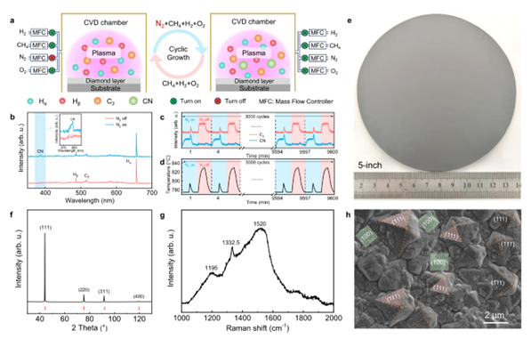
Figure 1 Diamond wafer prepared using the microwave plasma chemical vapor deposition (MPCVD) method.
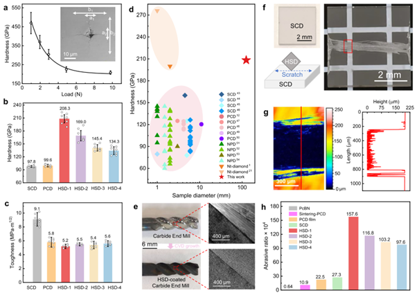
Figure 2 Mechanical properties of ultrahard diamond and their comparison with other diamonds.
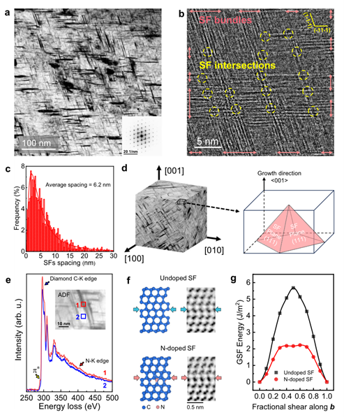
Figure 3 Microscopic structure and hardening mechanism of high-density stacking-fault diamond.
Article link:
https://www.nature.com/articles/s41467-025-66456-7
About Professor Yang Lu
Professor Yang Lu is currently Chair Professor of Nanomechanics in the Department of Mechanical Engineering and Kingboard Professor in Materials Engineering, and serves as Associate Dean (Mainland Affairs) of the Faculty of Engineering. Professor Lu is a leading expert in experimental nanomechanics and its interdisciplinary applications in materials engineering, advanced manufacturing, and semiconductor technologies. He is recognized for his groundbreaking works on elucidating the extreme mechanical properties of crystalline solids at micro- and nanoscale, and his innovative use of nanomechanics to manipulate micro/optoelectronics and their applications in a diverse set of engineering areas. Professor Lu has published more than 300 journal articles in peer-reviewed academic journals including Science, Nature Materials, Nature Nanotechnology etc., 2 book chapters and 7 US patents granted.