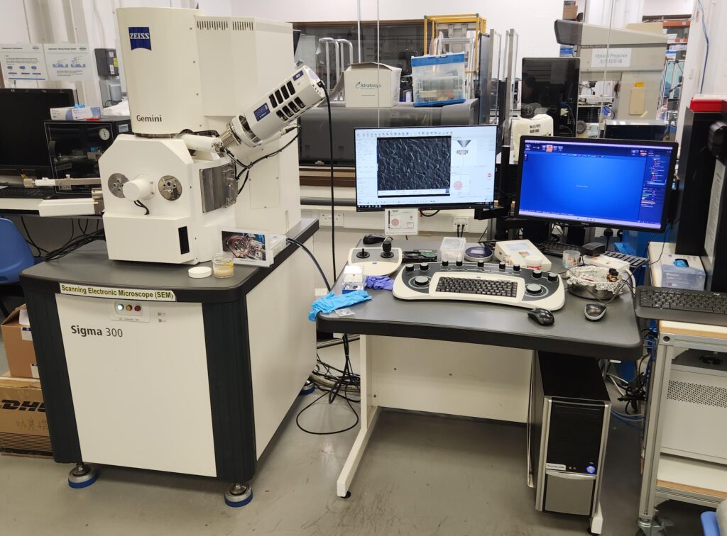
The Sigma 300 SEM, from Zeiss, is a field emission scanning electron microscope. It offers ultra-high resolution for both SE to image surface information and BSE to present compositional information in the high vacuum mode. In addition, EBSD and EDS imaging modes are available to obtain crystal orientation and chemical composition information of samples. A variety of in-situ experiments can be performed during imaging, including tensile tests and nano-indentation experiments.
Detectors:
• SE2 and InLens – Secondary Electron Detectors
• BSD – Backscatter Electron Detector
• EBSD Aztec Symmetry NANOANALYSIS WITH Fast & High Sensitive CMOS Camera, Maximum Indexing rate 3000HZ
• Energy Dispersive Spectroscopy (EDS) detector
Remarks: Under user-pay principle, the users or their supervisors should allocate budget for using the equipment. The detailed charging scheme can be found in https://mech.hku.hk/mech_facility_charging/. To apply for usage right(s), please visit the Moodle page: https://mech.hku.hk/admin_n_safety, or contact the laboratory technician, Mr Patrick Ng (email: patckng@hku.hk), for assistance.
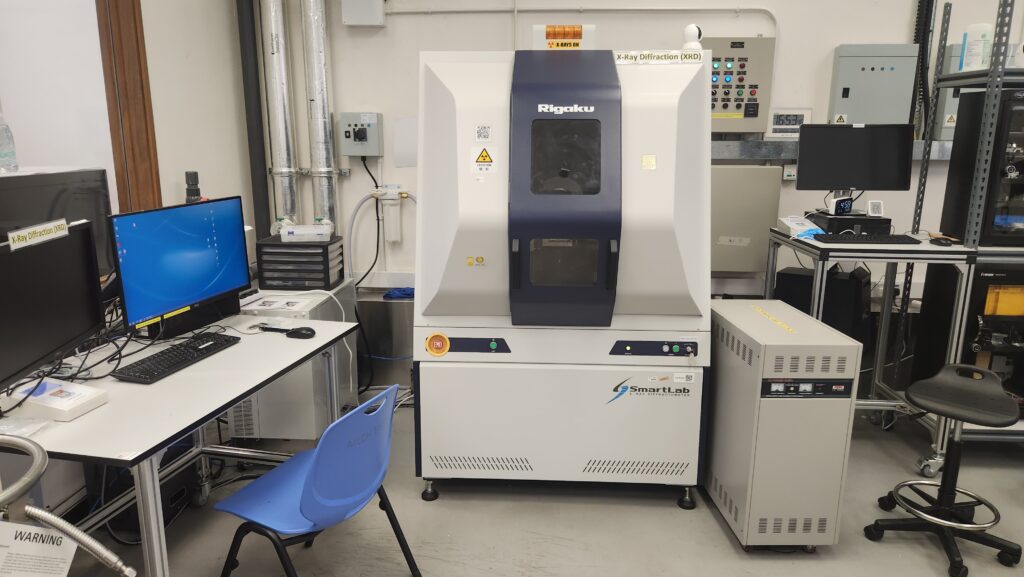
Rigaku SmartLab is a XRD system which can obtain the structure of materials at atomic or molecular level. The diffraction pattern provides information such as atomic structures, lattice parameter and chemical bonds. Applications of XRD include phase determination, crystallography, pharmaceutical research, semiconductor defects, strain, stress analysis, etc. Materials studies vary from salts, metals, minerals, semiconductors thin films, organic, inorganic, nanomaterials, biological molecules, etc.
Specifications / Applications:
• 9 kW high power X-ray generator
• Micro-area X-ray diffraction measurements (X-ray spot size down to 300um diameter)
• Automatic 8 position powder sample changer with spinner
• Full automated alignment under computer control.
• The system incorporates a high resolution θ/θ closed loop goniometer drive system, cross beam optics (CBO), an in-plane scattering arm, and an optional 9.0 kW rotating anode generator.
• Focusing and parallel beam geometries without reconfiguration.
• SAXS capabilities.
Remarks: Under user-pay principle, the users or their supervisors should allocate budget for using the equipment. The detailed charging scheme can be found in https://mech.hku.hk/mech_facility_charging/. To apply for usage right(s), please visit the Moodle page: https://mech.hku.hk/admin_n_safety, or contact the laboratory technician, Mr Patrick Ng (email: patckng@hku.hk), for assistance.
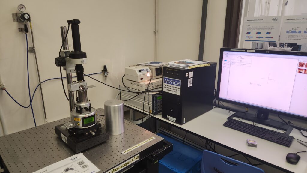
The Bruker MultiMode 8 AFM provides nano-meter surface topography imaging and pico-Newtown surface force measurement in both air and liquids. Bruker’s exclusive ScanAsyst mode offers automatic image optimization for faster, more consistent results. It will continuously adjust scan rate, setpoint and gains to obtain the highest quality image. Imaging in fluid has never been easier. There’s no need for cantilever tuning and ScanAsyst continuously monitors the tip-sample interaction force, thereby eliminating setpoint drift. PeakForce QNM enables direct mapping of nanomechanical properties, including elastic modulus, adhesion and dissipation, at high resolution and normal scan rates. The data channels are quantitative and unambiguous, unlike conventional phase imaging and some competing multi-frequency techniques.
Specifications / Applications:
• Contact, Tapping, and ScanAsyst imaging modes
• Normal and lateral forces measurement
• AFM resolution: < 5 nm
• No additional sample treatment needed
• Chemical-electric measurement module
Remarks: Under user-pay principle, the users or their supervisors should allocate budget for using the equipment. The detailed charging scheme can be found in https://mech.hku.hk/mech_facility_charging/. To apply for usage right(s), please visit the Moodle page: https://mech.hku.hk/admin_n_safety, or contact the laboratory technician, Mr Patrick Ng (email: patckng@hku.hk), for assistance.
Setaram Labsys Evo is a thermogravimetric analyzer. It has a wide range of applications for DSC/DTA, TGA, simultaneous TGA-DSC/DTA, Cp measurements. Various fields of application are possible including polymers and plastics, advanced materials, pharmaceutical compounds, inorganic substances, thermodynamics (Specific Heat Capacity Cp precision within 2 %), energy, etc.
Its wide temperature range is: from 25 ° C to 1600 ° C
Gas type: UHP Argon, UHP Nitrogen

Remarks: Under user-pay principle, the users or their supervisors should allocate budget for using the equipment. The detailed charging scheme can be found in https://mech.hku.hk/mech_facility_charging/. To apply for usage right(s), please visit the Moodle page: https://mech.hku.hk/admin_n_safety, or contact the laboratory technician, Mr Patrick Ng (email: patckng@hku.hk), for assistance.
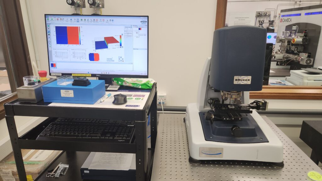
The Bruker Contour GT-K Automated System is an optical profiler that utilizes white light interferometry to aid researchers in 3D non-contact surface metrology studies. It divides a beam of light from a single source into two, directs one of them onto the sample surface, and then recombines the beams to create an interference pattern. By measuring the path difference between the two beams, the sample surface profile can be obtained with high degree of vertical resolution
Specifications / Applications:
PSI, VSI, VXI modes
- Stitching function available
- Accurate and repeatable throughout the 10mm scan range
- Patented dual LED illumination
- 5X and 10X interferometric objectives
- 5X, 10X and 20X interferometric objectives
- Thick film measurement capability
- AcuityXR enhanced resolution measurement mode (including HDVSI)
Remarks: Under user-pay principle, the users or their supervisors should allocate budget for using the equipment. The detailed charging scheme can be found in https://mech.hku.hk/mech_facility_charging/. To apply for usage right(s), please visit the Moodle page: https://mech.hku.hk/admin_n_safety, or contact the laboratory technician, Mr Patrick Ng (email: patckng@hku.hk), for assistance.
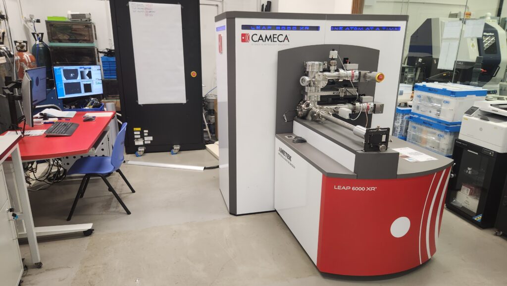
Cameca LEAP 6000 XR is an advanced 3D Atom Probe Tomography (APT) instrument designed for nanoscale materials analysis. This system is able to offer extensive capabilities for both 3D imaging and chemical composition measurements at the atomic scale (around 0.1-0.3nm resolution in depth and 0.3-0.5nm laterally). Since its early developments, Atom Probe Tomography has contributed to major advances in materials science.
The sample is prepared in the form of a very sharp tip. The cooled tip is biased at high DC voltage (3-15 kV). The very small radius of the tip and the High Voltage induce a very high electrostatic field (tens V/nm) at the tip surface, just below the point of atom evaporation. Under laser or HV pulsing, one or more atoms are evaporated from the surface, by field effect (near 100% ionization), and projected onto a Position Sensitive Detector (PSD) with a very high detection efficiency. Ion efficiencies are as high as 80%, the highest analytical efficiency of any 3D microscopy.
Cameca LEAP 6000 XR APT inherits key features from previous APT generations, adding deep UV laser pulsing to the proven local electrode design to deliver higher yield and data quality. Through compatibility with the microtip array and a redesigned optical system, the LEAP 6000 XR provides enhanced ease of use and the potential for fully automated operation.
Remarks: Under user-pay principle, the users or their supervisors should allocate budget for using the equipment. The detailed charging scheme can be found in https://mech.hku.hk/mech_facility_charging/. To apply for usage right(s), please visit the Moodle page: https://mech.hku.hk/admin_n_safety, or contact the laboratory technician, Dr Patrick Ng (email: patckng@hku.hk), for assistance.
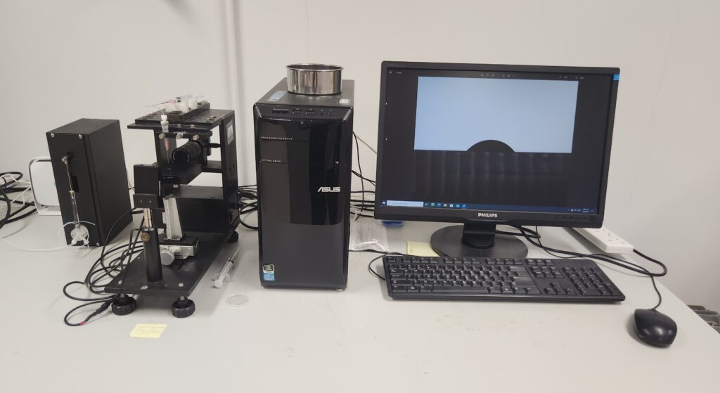
The Sindatek Model 100SB is a video-based contact angle meter. It consists of the basic hardware with the following technical features:
• Basic platform with needle holder and syringe support
• Homogeneous LED backlighting electronics with continuously adjustable intensity
• Measuring stage, adjustable in three axis for the accurate sample positioning
• Adjustable tilt optics
• Fixed lens with optional high-performance lens with an integrated continuous fine focus
• High resolution 1280 x 1024 USB 2.0 camera; optional 60 fps speed camera
• Manual dosing unit with fine 1.0 ul adjustable syringe
• Integral X-Y-Z fine adjustable needle holder
Remarks: Under user-pay principle, the users or their supervisors should allocate budget for using the equipment. The detailed charging scheme can be found in https://mech.hku.hk/mech_facility_charging/. To apply for usage right(s), please visit the Moodle page: https://mech.hku.hk/admin_n_safety, or contact the laboratory technician, Dr Patrick Ng (email: patckng@hku.hk), for assistance.
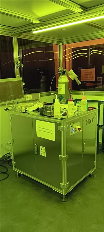
MNT-S100Oz-L4 is an atomic layer deposition system, which can control the formation of high-quality, ultra-thin films with atomic-level precision. The MNT-S100Oz-L4 ALD system is specifically designed for the deposition of high-k dielectric materials such as HfO₂ (hafnium oxide) and Al₂O₃ (aluminum oxide), achieving film thicknesses in the range of 10–30 nm. ALD technology offers exceptional control over film thickness and uniformity, making it well-suited for semiconductor device fabrication, nanotechnology research, and advanced material development. Specifications / Applications:
• Deposition of high-k dielectric materials: HfO₂ and Al₂O₃
• Precise thickness control: 10–30 nm
• Superior film uniformity across substrates
• Suitable for semiconductor device fabrication
• Applicable in advanced material and nanotechnology research
Remarks: Under user-pay principle, the users or their supervisors should allocate budget for using the equipment. The detailed charging scheme can be found in https://mech.hku.hk/mech_facility_charging/. To apply for usage right(s), please visit the Moodle page: https://mech.hku.hk/admin_n_safety, or contact the laboratory technician, Dr Patrick Ng (email: patckng@hku.hk), for assistance.
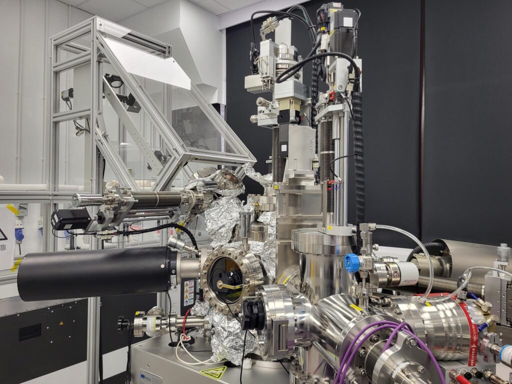
The Pulsed Laser Deposition (PLD) system is designed for developing high-quality, large-area ultra-high dielectric constant insulators. It integrates advanced femtosecond laser transient absorption spectroscopy for precise and high-quality film deposition. Specifications / Applications:
- Femtosecond Laser Transient Absorption Spectroscopy System
- Components:
- PH2-20W: High-power femtosecond laser
- ORPHEUS-HP: Optical parametric amplifier (OPA)
- ORPHEUS-HP-SH: Second harmonic generation module
- HELIOS VIS: Transient absorption spectroscopy system
- Microscope (SGL SPOT+REFLECTION ADDON)
- Applications:
- Development of ultra-high dielectric constant insulators
- High-quality, large-area film deposition for electronics
- Materials science, nanotechnology, and semiconductor research
- Fabrication of high-k dielectric materials (capacitors, transistors)
Real-time monitoring and analysis of film properties
Remarks: Under user-pay principle, the users or their supervisors should allocate budget for using the equipment. The detailed charging scheme can be found in https://mech.hku.hk/mech_facility_charging/. To apply for usage right(s), please visit the Moodle page: https://mech.hku.hk/admin_n_safety, or contact the laboratory technician, Dr Patrick Ng (email: patckng@hku.hk), for assistance.
The LAMBDA™ 365 is an UV-Vis spectrometer. It delivers a variable spectral bandwidth capability from 0.5 nm to 20 nm, the operation range is between 190-1100 nm, to meet your application needs. It can accommodate a wide range of accessories, including multicell changers, solid sample accessories for transmission, reflectance, and a range of cuvette holders to meet your sampling requirements.
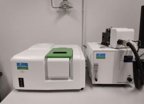
Remarks: Under user-pay principle, the users or their supervisors should allocate budget for using the equipment. The detailed charging scheme can be found in https://mech.hku.hk/mech_facility_charging/. To apply for usage right(s), please visit the Moodle page: https://mech.hku.hk/admin_n_safety, or contact the laboratory technician, Dr Patrick Ng (email: patckng@hku.hk), for assistance.
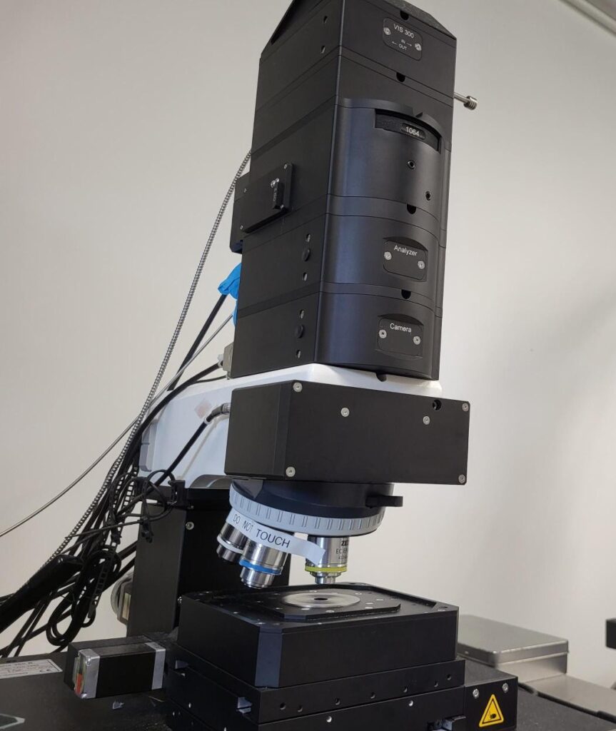
The Integrated Confocal Raman Mapping Microscope System is equipped with a WITec multiwavelength (488nm) laser coupler, a high-precision microscope base, and a selection of high-quality objectives (10x, 50x, 100x, and 50x with NA=0.55). This advanced high-resolution Raman and photoluminescence (PL) mapping system is further enhanced with a temperature control unit, enabling detailed chemical and structural analysis of materials at the microscale. It is an essential instrument for cutting-edge research in materials science, chemistry, and nanotechnology. Specifications / Applications:
- High-resolution confocal Raman and PL mapping capabilities
- Integrated WITec multiwavelength laser coupler for versatile excitation options
- Microscope base with high stability and precision control
- Temperature control system for accurate sample environment management
- Ideal for detailed chemical and structural analysis of materials
- Applications in materials science, chemistry, nanotechnology, and more
Enables the study of material properties, phase identification, and stress/strain analysis
Remarks: Under user-pay principle, the users or their supervisors should allocate budget for using the equipment. The detailed charging scheme can be found in https://mech.hku.hk/mech_facility_charging/. To apply for usage right(s), please visit the Moodle page: https://mech.hku.hk/admin_n_safety, or contact the laboratory technician, Dr Patrick Ng (email: patckng@hku.hk), for assistance.
Our Fused Deposition Modeling (FDM) 3D printing suite provides students, faculty, and researchers with robust rapid prototyping capabilities. Whether you are iterating early-stage design concepts or manufacturing highly durable functional parts, our equipment is tailored to support a wide array of academic and research applications.
A standout feature of our facility is the advanced multi-material capability, which supports printing with up to 8 distinct filaments in a single job. This allows for complex geometries using breakaway or soluble support materials, as well as the creation of multi-material models for detailed engineering designs and visual presentations.
Available models:
- 2 × Bambu Lab X1 Carbon
- 3 × Bambu Lab H2D
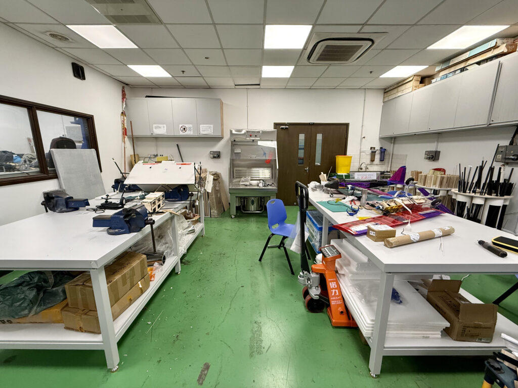
Our dedicated prototyping facilities, located at G/F, Haking Wong Building, empower students and researchers to transform concepts into tangible realities. Primarily designed to enhance undergraduate learning and project development, these labs also support diverse university research initiatives. Our comprehensive resources include advanced machinery and a well-equipped workshop for hands-on fabrication.
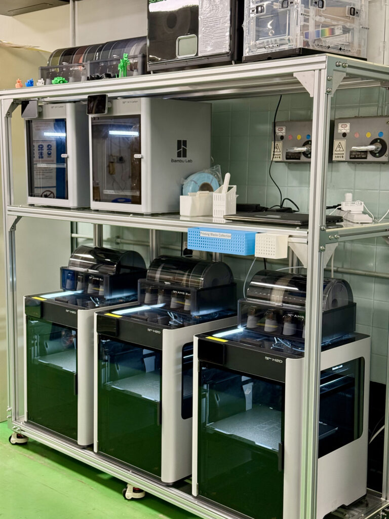
Remarks: Users must bring their own RFID-enabled printing filament. Authorization and training are mandatory for self-operation.
Our facility features an industrial-grade Thunder Laser system capable of high-precision cutting and intricate engraving. Ideal for rapid manufacturing and iterative design, this machine allows students and researchers to quickly fabricate custom components and models prior to final assembly. The system is highly versatile, supports a wide range of materials, and easily accommodates large-scale workpieces or high-volume batch production.
Specifications:
- Supported Materials: Various woods, plastics, and acrylics
- Max Working Area: 1300 × 900 mm
Our dedicated prototyping facilities, located at G/F, Haking Wong Building, empower students and researchers to transform concepts into tangible realities. Primarily designed to enhance undergraduate learning and project development, these labs also support diverse university research initiatives. Our comprehensive resources include advanced machinery and a well-equipped workshop for hands-on fabrication.
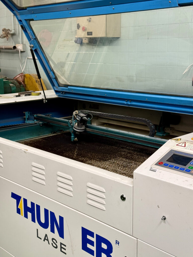
Remarks: Users must bring their own workpieces. Authorization and training are mandatory for self-operation.
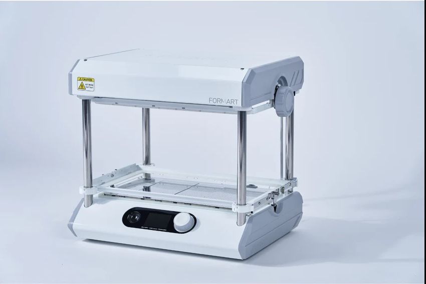
The lab utilizes a FORMART 2 Pro vacuum former to produce highly detailed prototypes and custom molds through the process of thermoforming. It provides a fast and effective method for shaping heated thermoplastic sheets into precise physical forms. Engineered to support substantial project dimensions, the system accommodates workpieces up to 470 × 270 mm.
Our dedicated prototyping facilities, located at G/F, Haking Wong Building, empower students and researchers to transform concepts into tangible realities. Primarily designed to enhance undergraduate learning and project development, these labs also support diverse university research initiatives. Our comprehensive resources include advanced machinery and a well-equipped workshop for hands-on fabrication.
Remarks: Users must bring their own workpieces. Authorization and training are mandatory for self-operation.
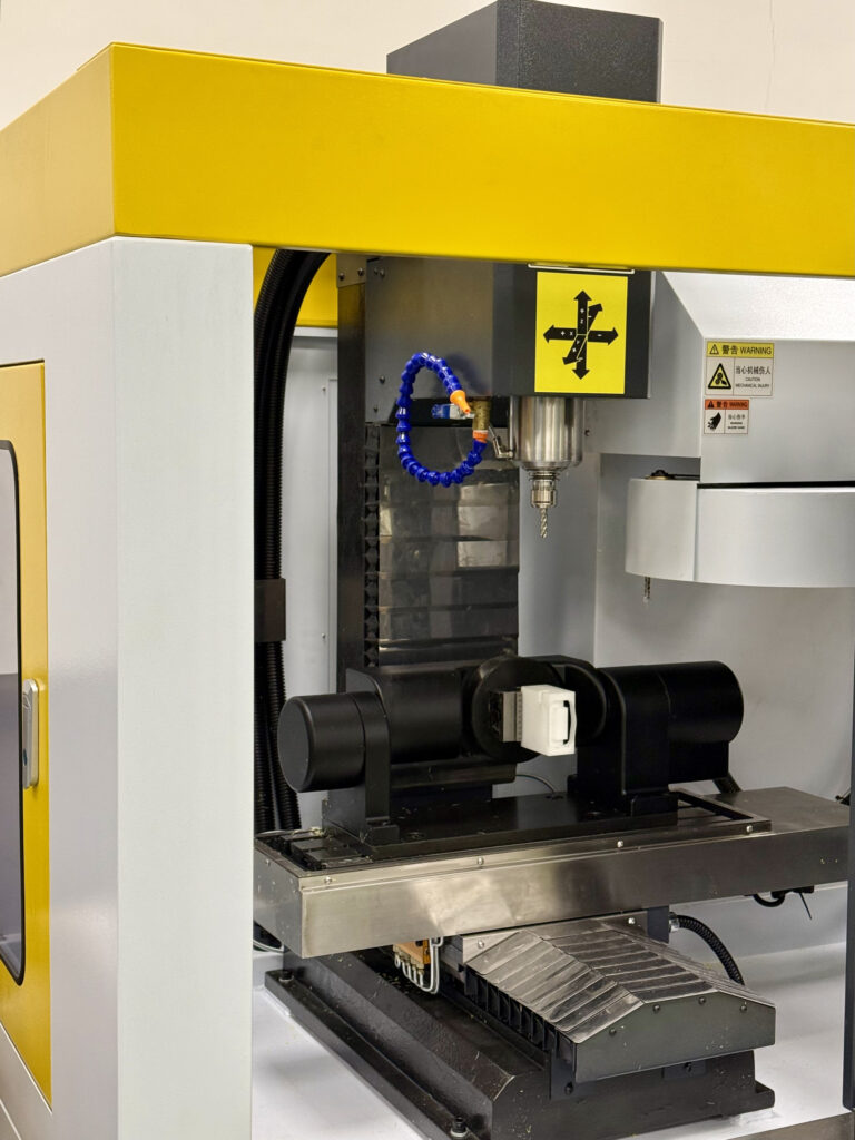
Our facility features a suite of advanced Computer Numerical Control (CNC) machines, offering precision subtractive manufacturing for creating high-accuracy components. These systems are essential for machining complex geometries, custom tooling, and functional mechanical prototypes from a diverse array of solid materials.
Available machines:
- 5-axis CNC mill: Capable of machining complex, multi-sided geometries and undercuts in a single setup. This machine processes non-ferrous metals (such as aluminum and brass), as well as various plastics and woods. It accommodates workpieces up to 150 × 150 × 80 mm.
- 3-axis CNC mill: Ideal for standard 2.5D and 3D profiling, pocketing, and contouring. This mill is dedicated to processing non-metallic workpieces (including woods, plastics, and tooling waxes) up to 50 × 100 × 50mm
- CNC lathe: Specialized for precision turning, threading, and creating complex cylindrical or rotational parts. It is designated for non-metallic workpieces with a maximum size of ⌀60 × 140mm
Our dedicated prototyping facilities, located at G/F, Haking Wong Building, empower students and researchers to transform concepts into tangible realities. Primarily designed to enhance undergraduate learning and project development, these labs also support diverse university research initiatives. Our comprehensive resources include advanced machinery and a well-equipped workshop for hands-on fabrication.
Remarks: Users must bring their own workpieces and tools . Authorization and training are mandatory for self-operation.